Lithography
The photolithography is in use to describe the set of operation for achieving a manufacturing process with the transfer of a pattern by light in a photo-sensitive resist. These photoresists are used to cover a part of the substrate for a subsequent process.
We are talking about non-permanent photosensitive resists often also called protective layers (or mask), stencil layers or molds. The processes that need a photosensitive resist are those:
- Plasma dry etching
- Chemical wet ecthing
- Material deposition (lift-off process)
- Electroplating
- Protective coating ... etc.
Depending on the process, the most suitable resist is chosen; we will mainly take into account its chemical properties, its polarity and its thickness. In addition, there are permanent resists used as end products to fabricate micro-components
(optic, fluidic or mechanics micro objects…). These are negative resist, thin or (very) thick.
But the first step where it all starts is the definition of the design by our optical mask generator. We manufacture a glass-chromium plate which will allow the reproduction in several copies of the patterns on the substrates.
Resource contact:
| Laurent ROBERT 03 81 66 66 47 lrobert [at] femto-st.fr | Personal page: https://www.femto-st.fr/fr/personnel-femto/laurentrobert |

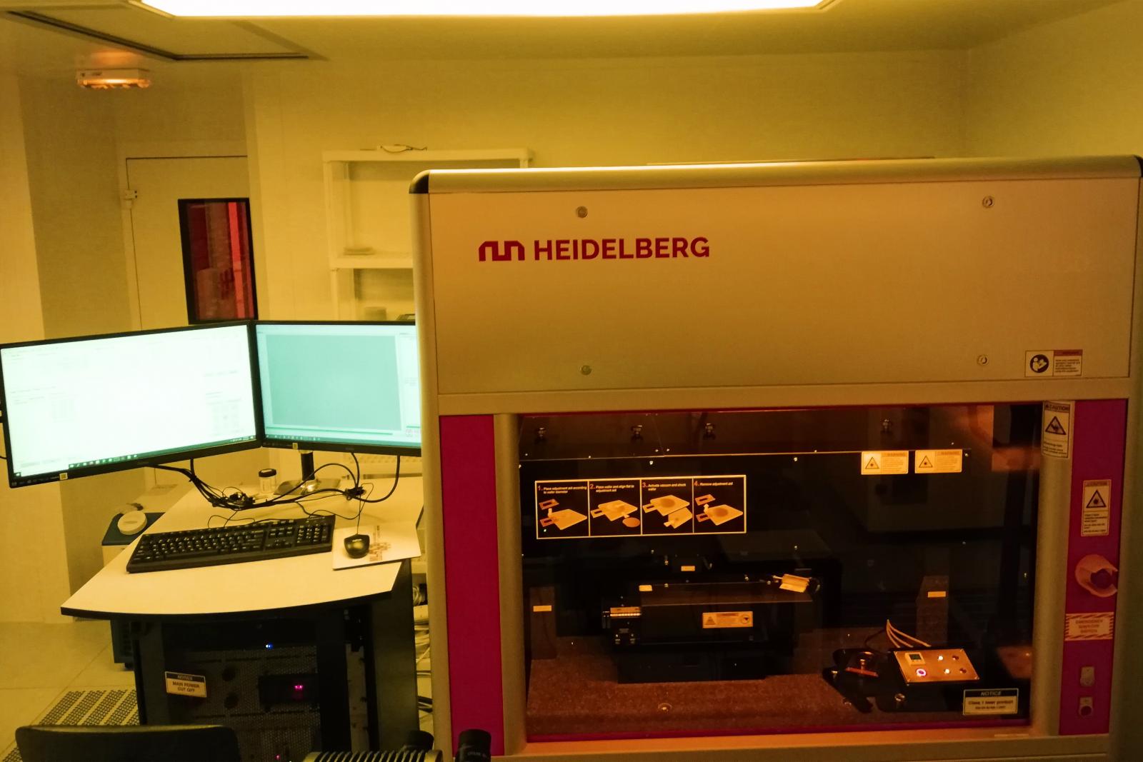
Optical mask generator
| HEIDELBERG MLA150 | Use: > Optical masks > Direct exposure > Grayscale lithography |
 | Technical specifications |
——
Semi automatic cleaning system
| Solar-Semi QS W300 | Use: > Mask & wafer cleaner |
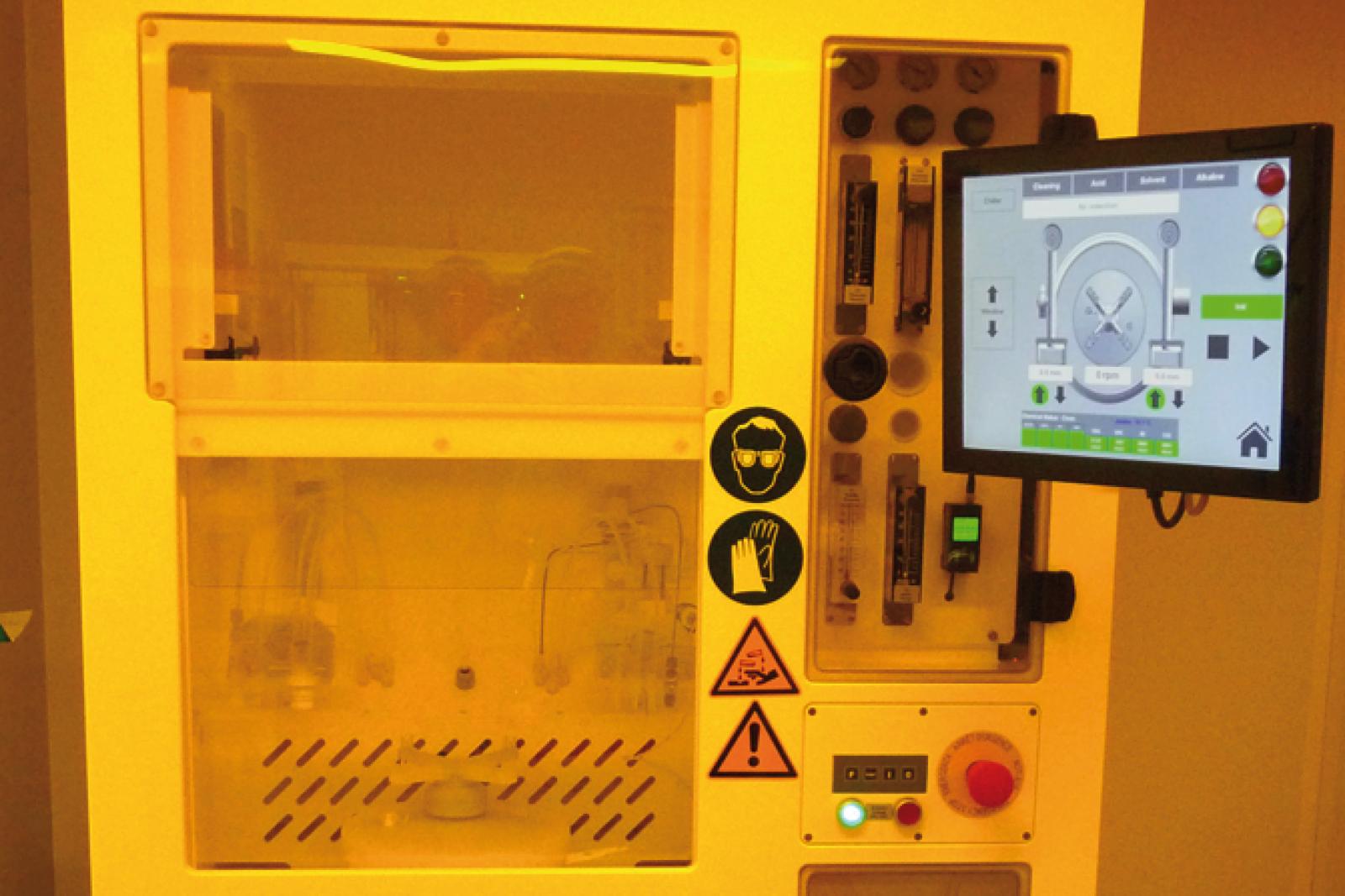 | Technical specifications |
——
Spin-coater with integrated hot plate
| Solar-Semi OC ST22 | Use: > Photoresists spin coating |
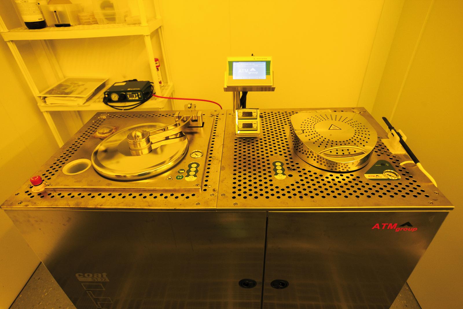 | Technical specifications |
——
Automatic spin-coater, baking and developer
| ACS 200 GEN3 | Use: > Adherence promotor > Photoresist coating > Photoresist development |
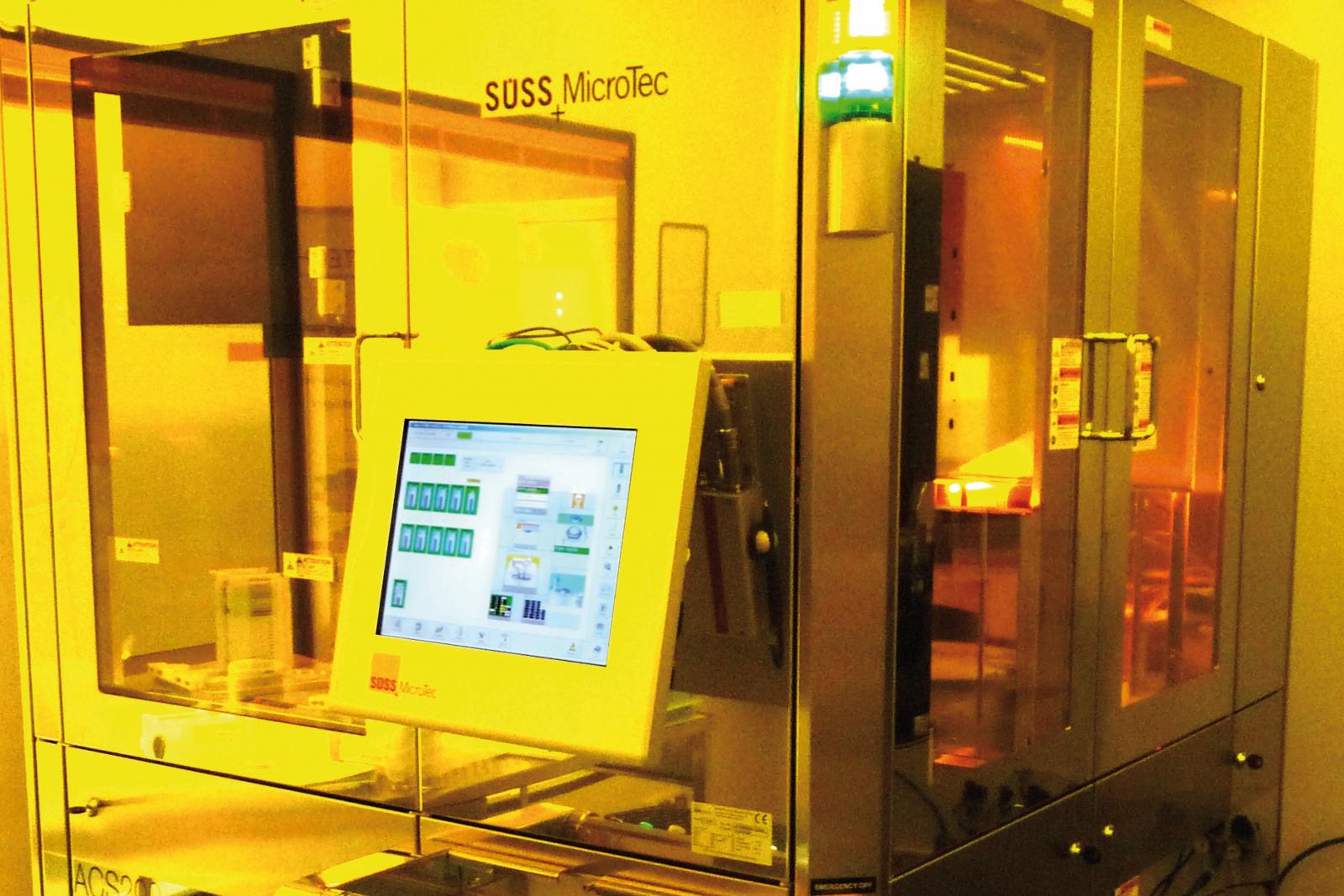 | Technical specifications |
——
Spray Coater
| Süss Microtec AS 8 | Use: > Conformal resist coating on substrate with high topology |
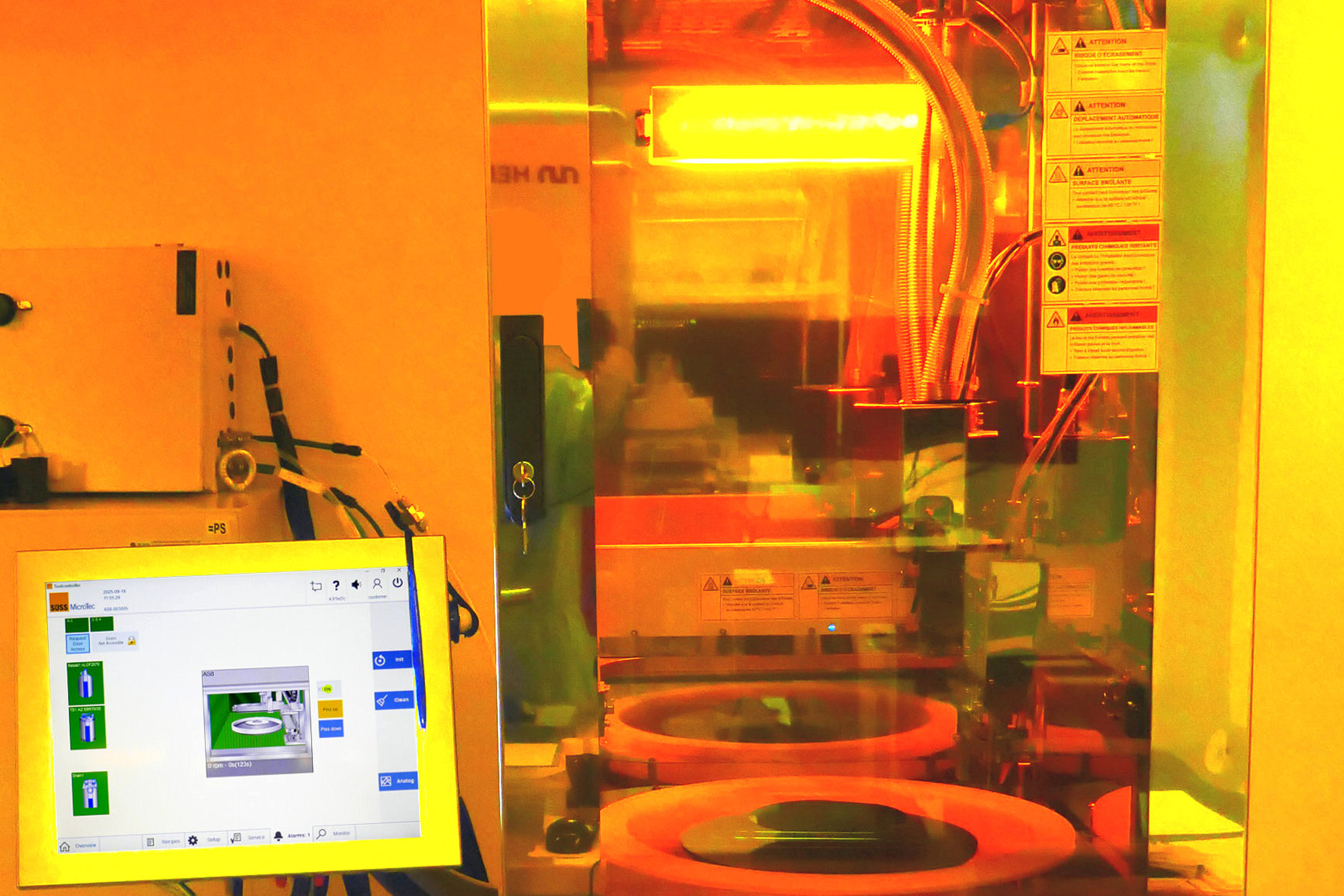 | Technical specifications |
——
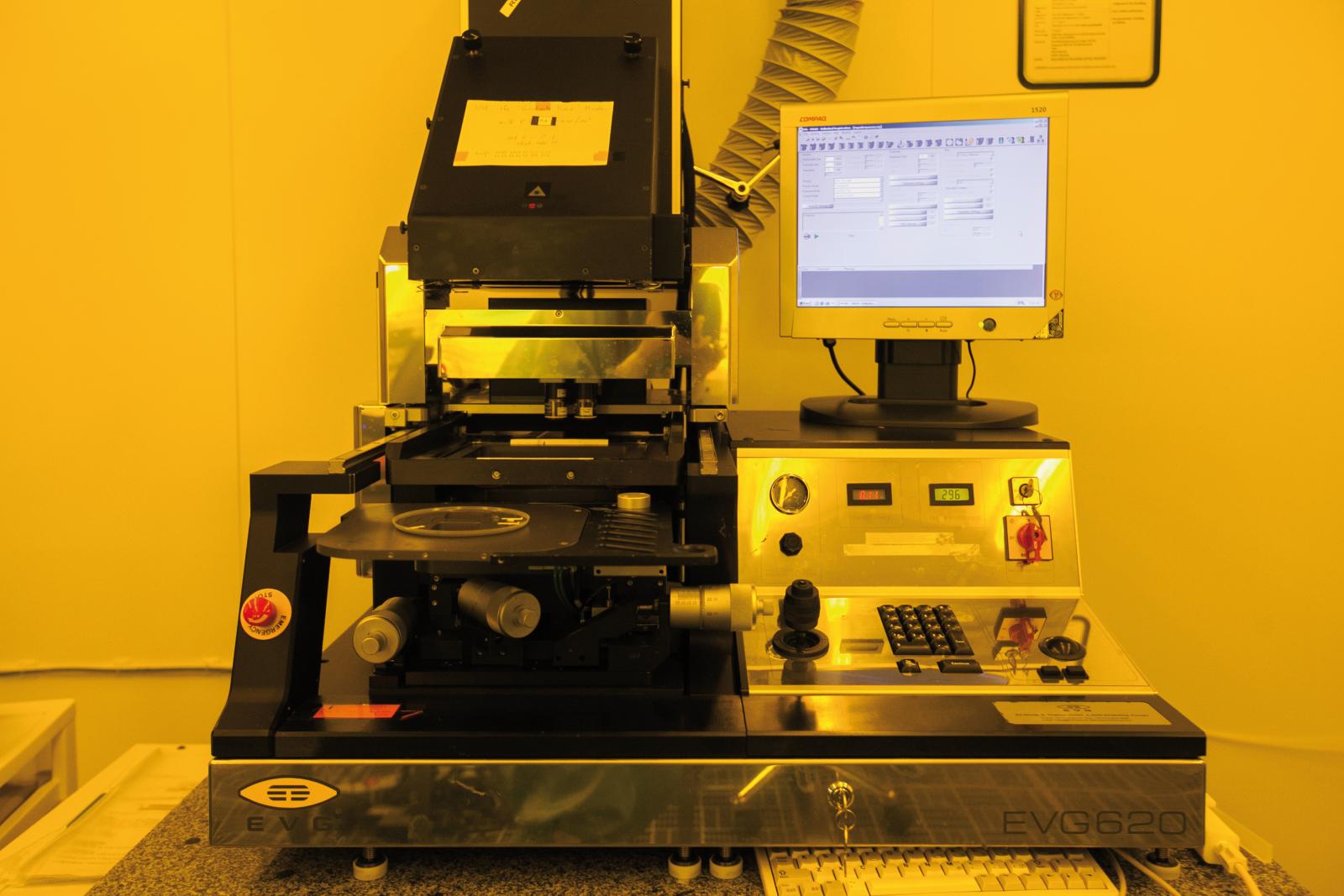
UV Double-side alignment system
| EVG 620 | Use: > Top and bottom side alignments > Alignment for bonding |
 | Technical specifications |
——
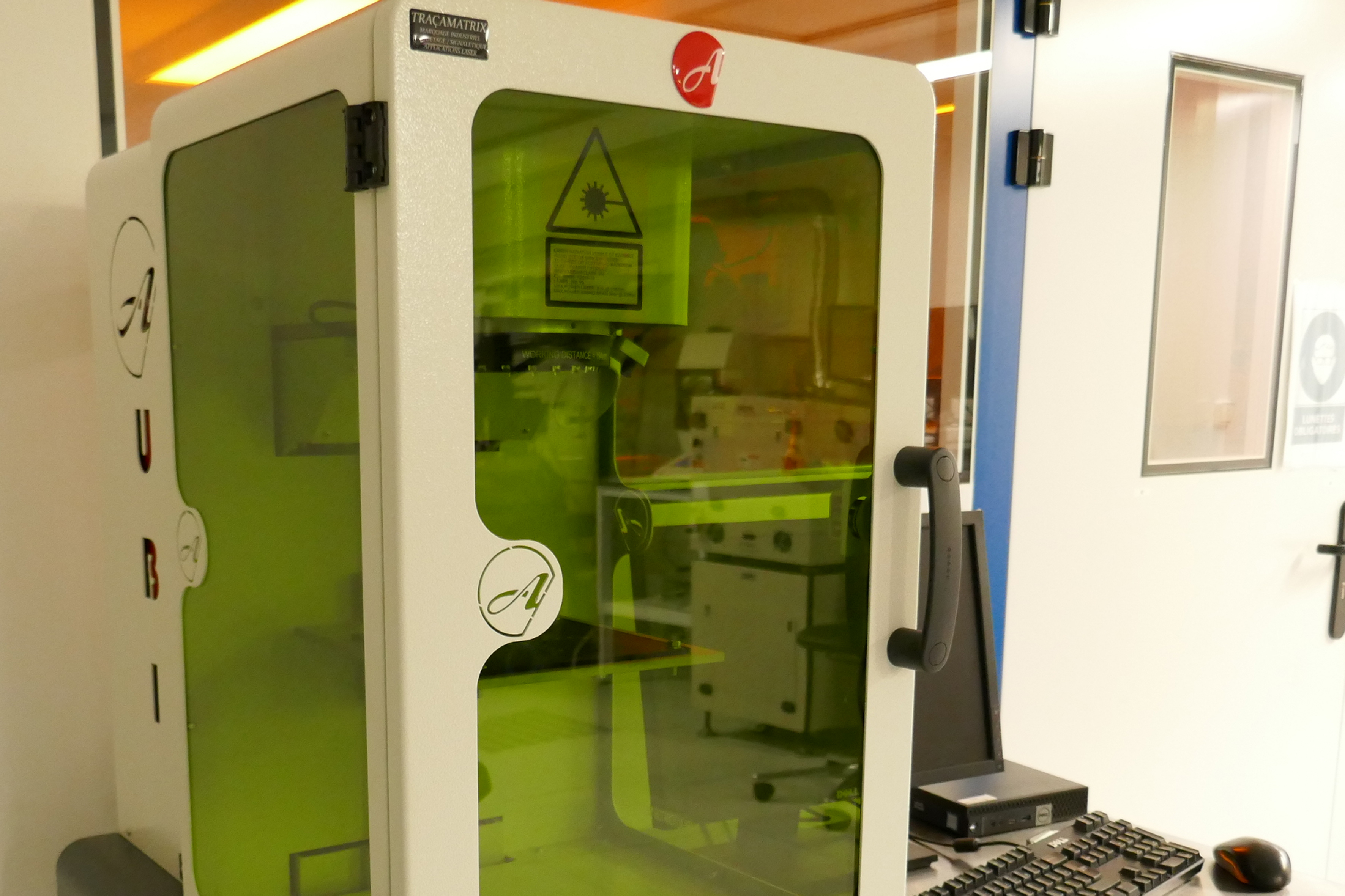
Laser marking system
| Traçamatrix | Use: > Wafer & device marking > Transparent & opaque |
 | Technical specifications |
——
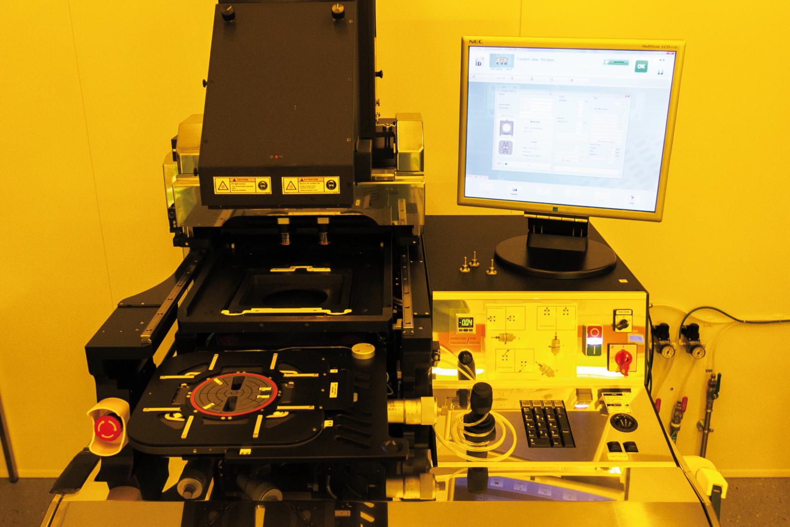
DUV Double-side alignment system
| EVG 620 | Use: > Top and bottom side alignments |
 | Technical specifications |
——
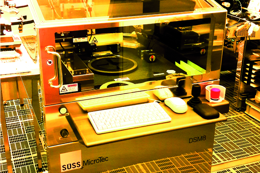
Semi-automatic metrology platform
| Süss Microtec DSM8 GEN2 | Use: > Top & bottom / Top & top Alignment control |
 | Technical specifications |
——
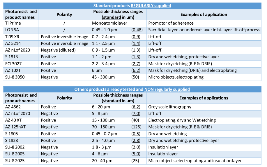
UV photoresists overview