Nanotechnology
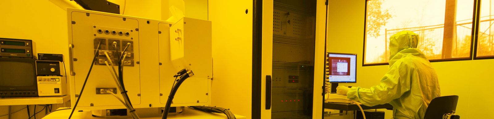
The Mimento facility has a dedicated resource to deal with structures of size below 1 µm. It is mainly composed of 2 high resolution equipments, namely an electron beam lithography station and a dual beam SEM (Scanning Electron Microscope) / FIB (Focused Ion Beam).
The electron beam lithography station is used for the exposition of electron sensitive resists. The feature size is in the range 20 nm - 1 µm and after development, the resist can be used as a mask for lift-off process or dry etching.
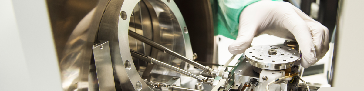
The dual beam can be used for different kind of process. The most common is for milling thanks to Ga ions, with a resolution down to 10 nm. It can also be used for local deposition (specific precursors) and for nano-manipulation (nano-robot). Characterization by cross-section (FIB milling and then SEM inspection of the slice) is a standard process and is very helpful for process optimization and MEMS’s behaviour understanding.
Resource contact:
| Roland SALUT 03 63 08 21 07 roland.salut [at] femto-st.fr | Personal page: https://www.femto-st.fr/fr/personnel-femto/rolandsalut |
| Marina RASCHETTI 03 63 08 26 56 marina.raschetti [at] femto-st.fr | Personal page: https://www.femto-st.fr/fr/personnel-femto/marinaraschetti |

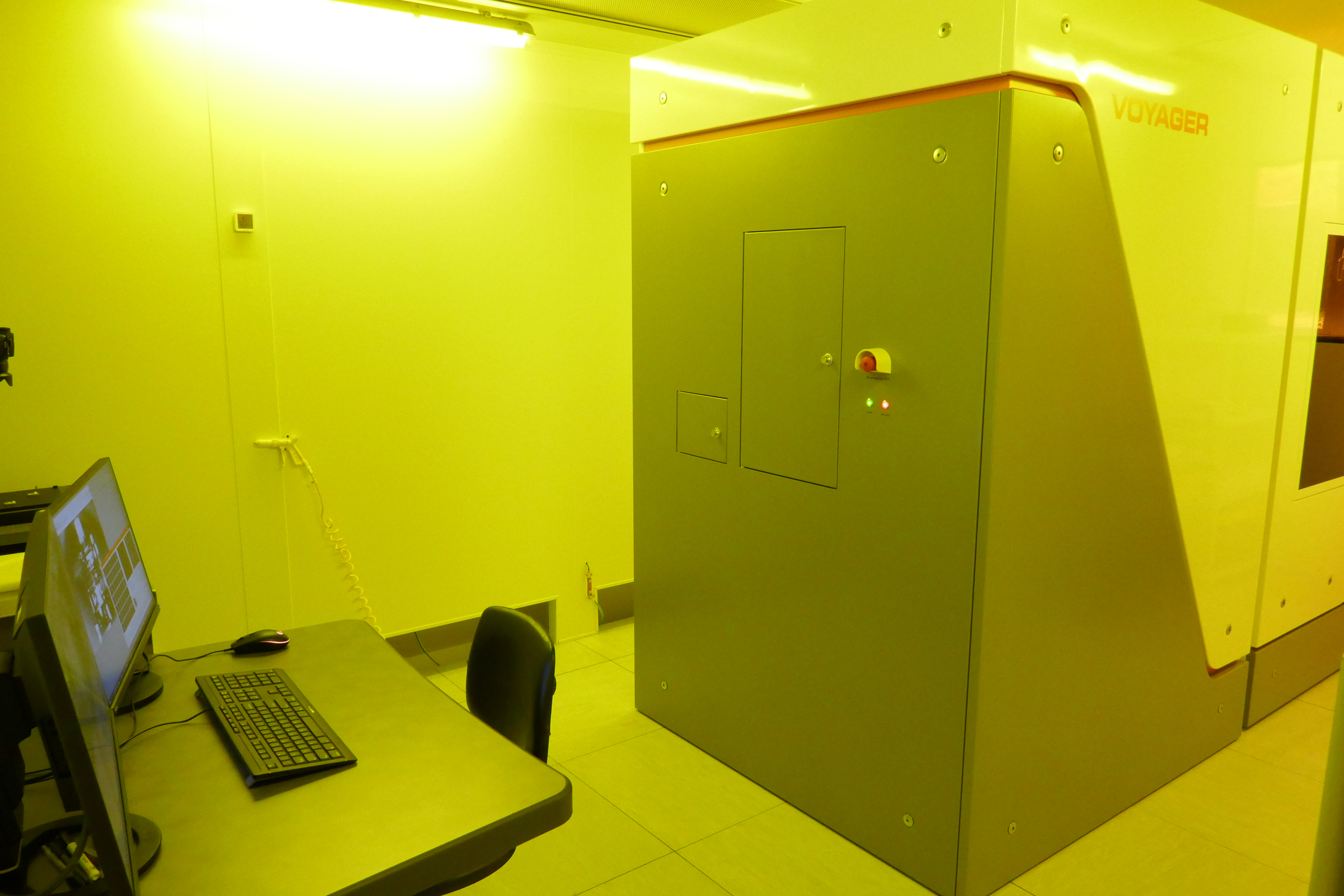
Electron beam lithography system
| Raith Voyager | Use: > Electronic lithography > Lift-off process > Mask for etching |
 | Technical specifications |
——
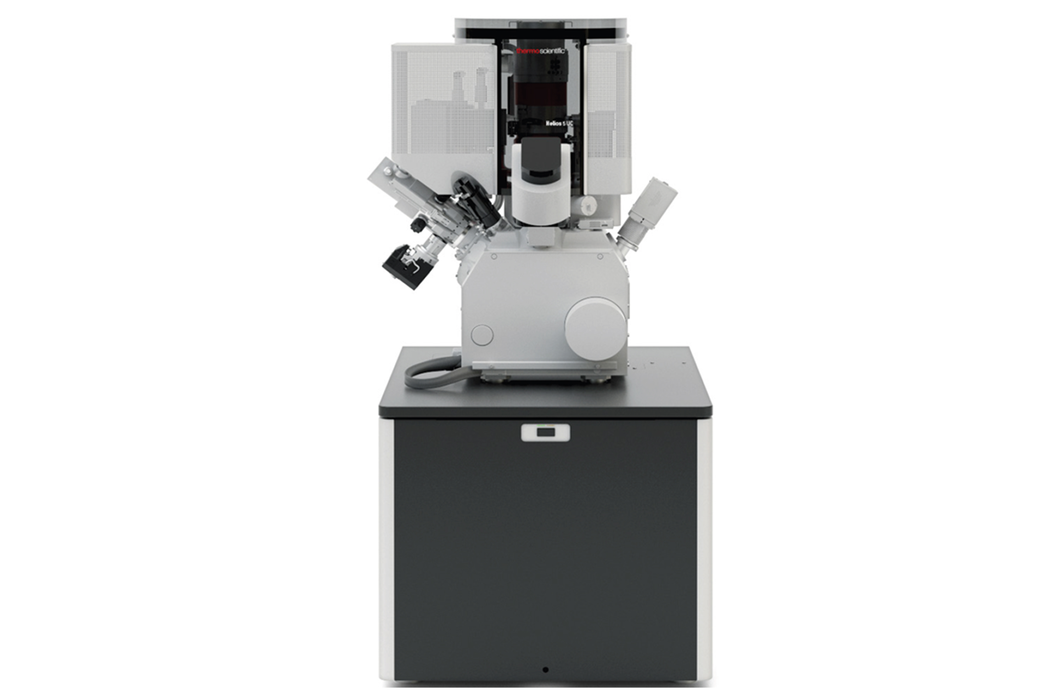
Focused Ion Beam system
| Thermo Fisher Scientific Helios 5 UC | Use: > Ion beam lithography > Cross section > SEM observation > 3D reconstruction |
 | Technical specifications |
——
Focused Ion Beam system
| Raith Velion | Use: > Ion beam lithography > Large area lithography > Ion implantation |
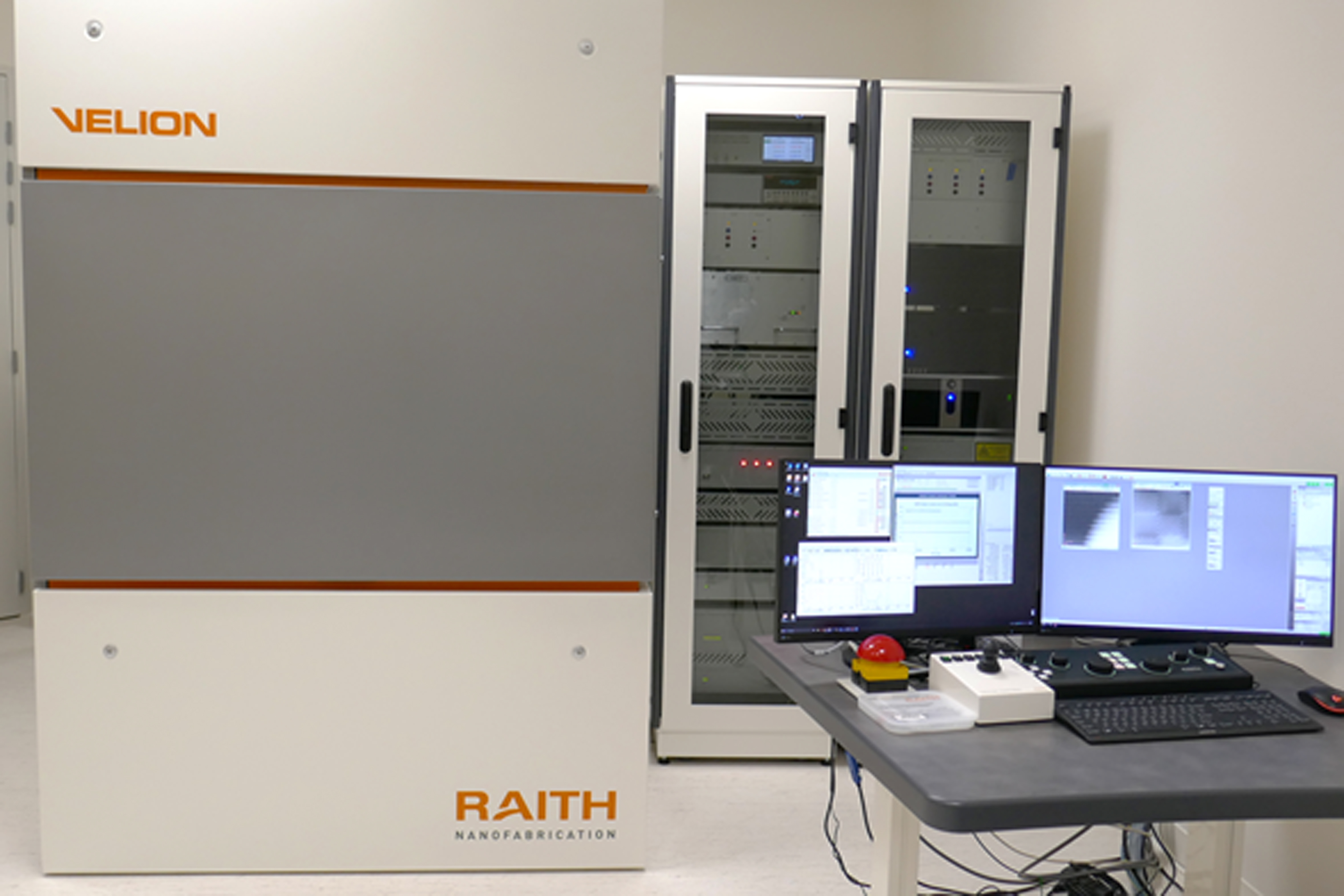 | Technical specifications |
——
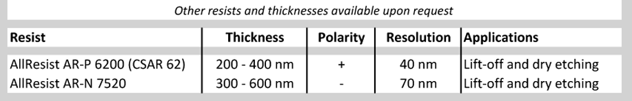
Electronic resists overview
——
Realisations
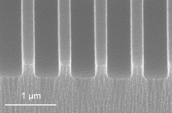 E-beam E-beamRIE etching of SiN | 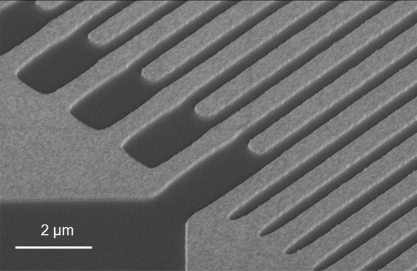 E-beam E-beamAluminium lift-off |
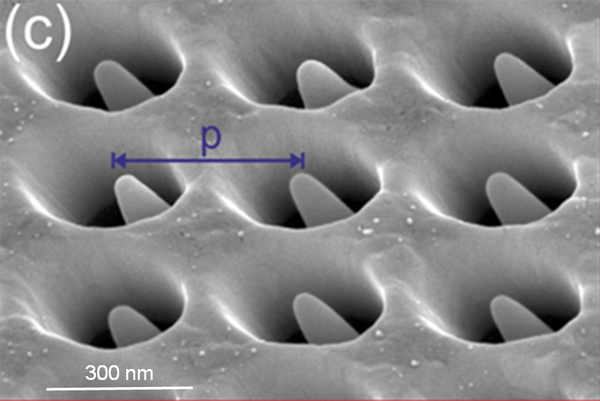 FIB FIBMilling with angle | 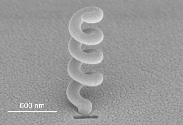 FIB FIB3D deposit |