This resource offers an access to several specialized tools dedicated to chip-level or wafer-level bonding and interconnection processes as well as to mechanical and optical characterization of bonding quality.
Chip-level packaging
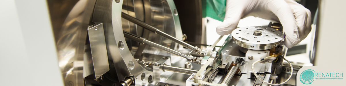
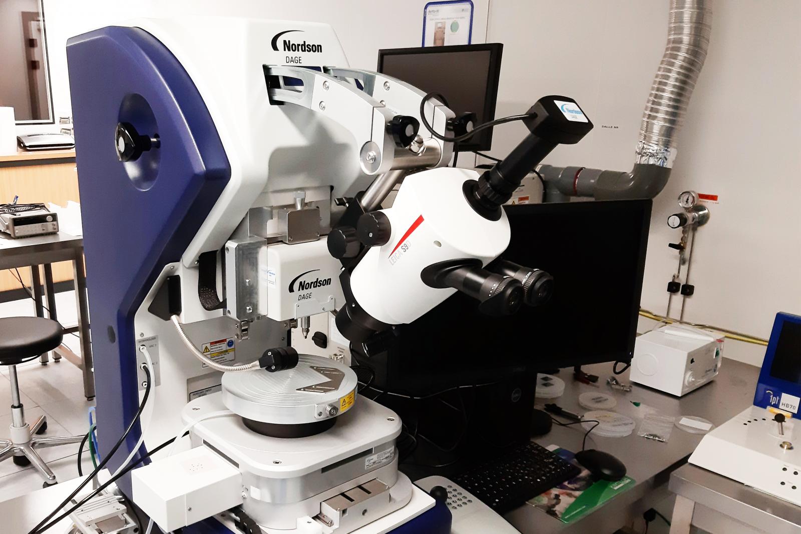
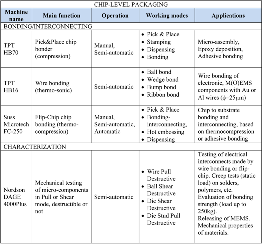
We ensure the traditional process flow, based on pick&place assembly of individual chips (TPT HB70), adhesive bonding with thermo- or electro-conductive epoxy (deposited by stamping or dispensing) and interconnection by wire bonding technique (TPT HB16). For higher performance packaging, we provide the flip-chip technology based on thermo-compression bonding (FC-250) and Au-based bumps. The quality of bonding can be evaluated with mechanical micro-bondtester (Nordson DAGE 4000Plus) in both pull or shear mode.
Wafer-level packaging
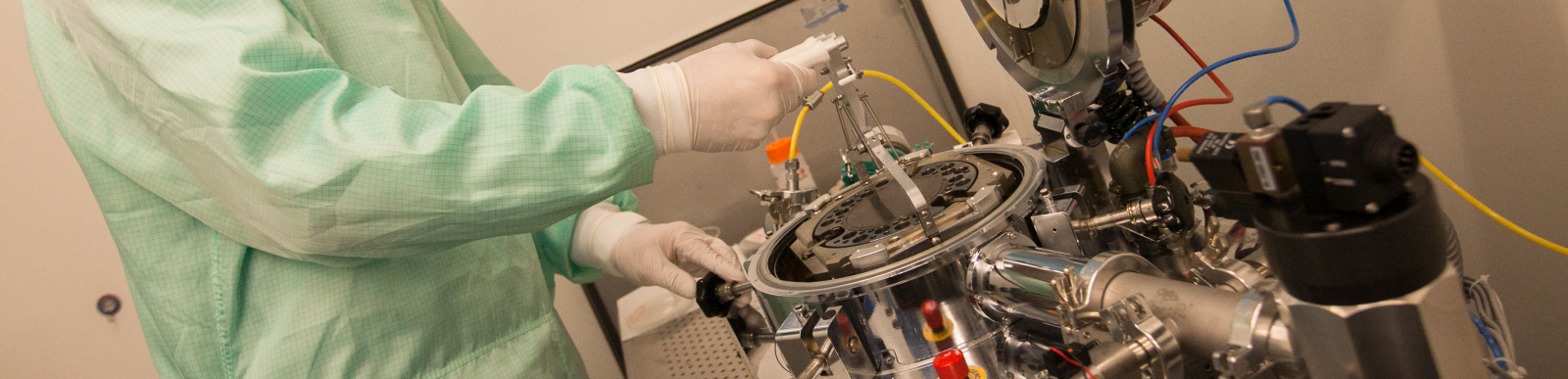
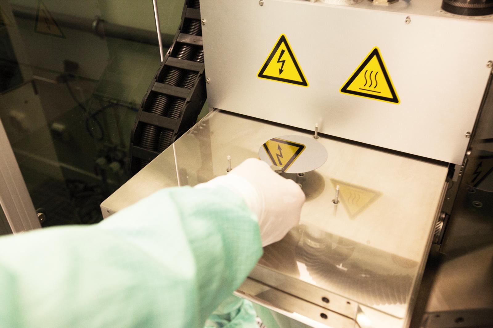
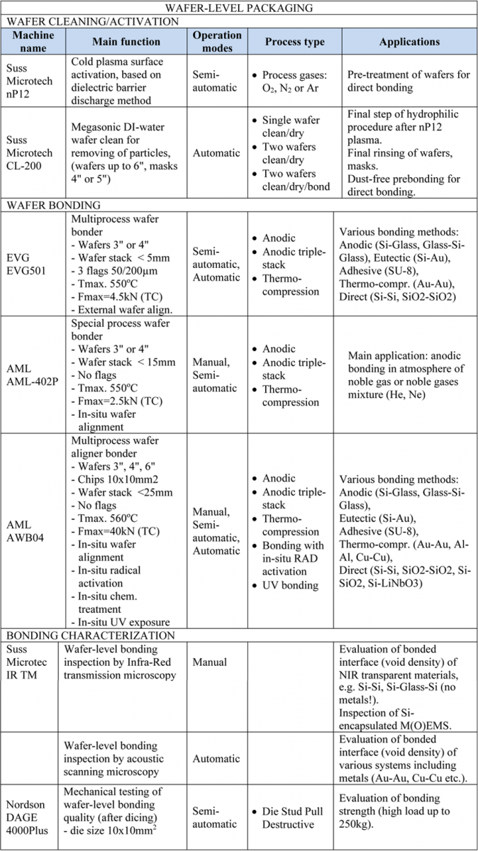
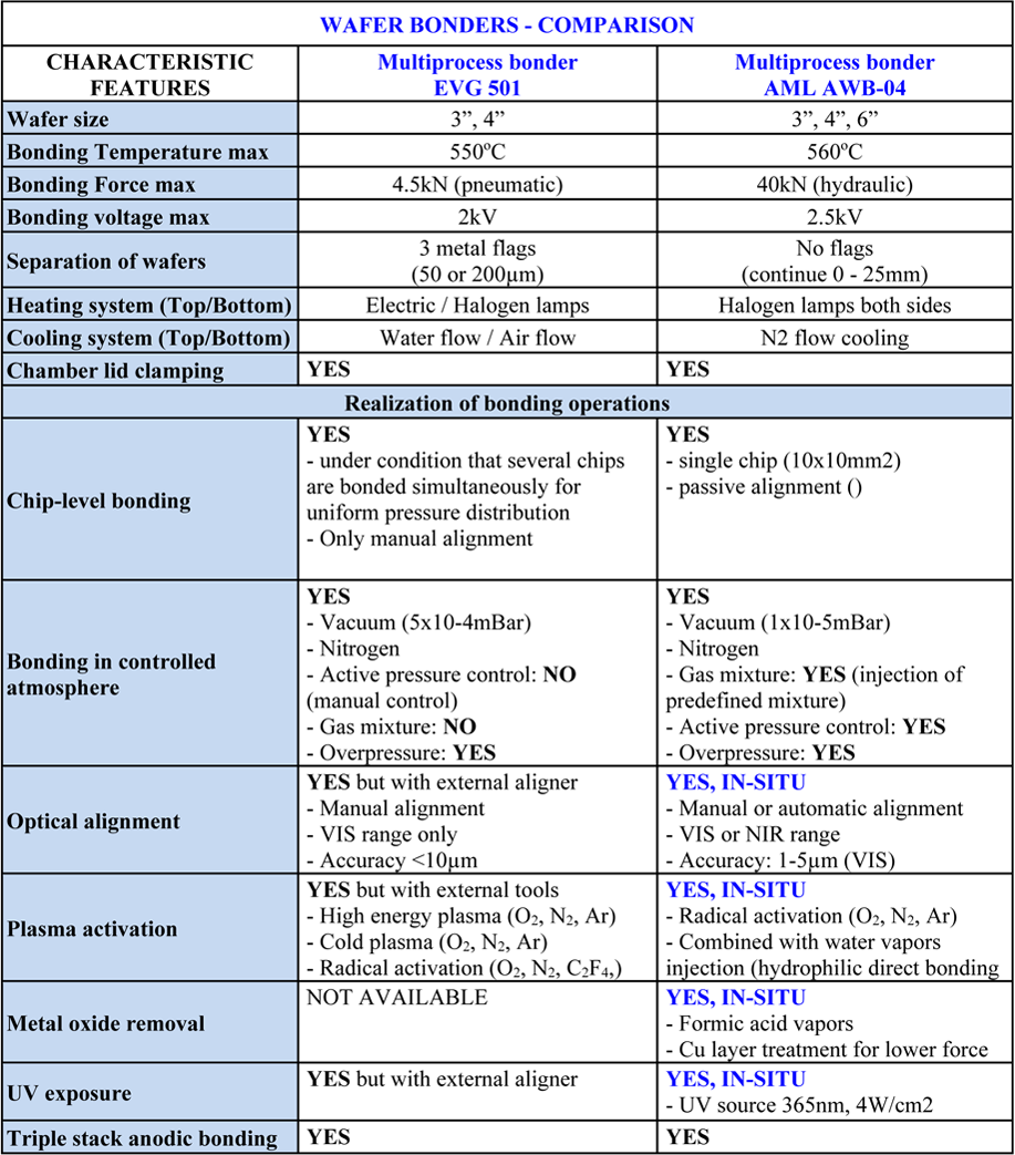
Several cleaning and surface activation processes are available to prepare the wafers for bonding, including fast cold plasma surface activation (Suss Microtec nP12) and megasonic DI-jet wafer cleaning/prebonding (Suss Microtec CL200). These tools can be combined with our versatile multi-process bonding systems (EVG501, AML-402P, AML AWB-04) allowing vertical wafer-level integration of heterogeneous components by medium/low temperature bonding (direct of indirect) up to 6" and bonding force up to 40kN. The distinguishing feature of the AWB-04 bonder is its ability to perform "in-situ" (i.e. in the same vacuum chamber) all key steps of a bonding process, i.e. wafer optical alignment (in VIS or IR range), surface plasma activation (O2, N2), vapor-based chemical treatment (H2O) or chemical etching of metal oxides (formic acid) as well as UV-exposure of polymer intermediate bonding layers.
Characterization methods
- Mechanical testing of bonded microcomponents and interconnections (Nordson DAGE 4000Plus).
Various tests (destructible or not) can be programmed in Pull or Shear modes. The wide range of load force (from 10g up to 250kg) and special micro-tools (hooks, blades etc.) allow number of applications, including optimization of wire/bump interconnection technology, evaluation of bonding quality or determination of material mech. properties. - Wafer-level inspection of bonding interface by Infra-Red transmission microscopy (IRTM).
IRTM method is rapid, non-destructive and non-contact, however only materials transparent in NIR spectrum can be observed (e.g. Si is translucent for NIR at l³1.2µm, metal layers are opaque). Moreover, IRTM offers several other advantages, i.e. real time observation, one-shot inspection of the entire wafer (max 4") and a good sensitivity to even small defects in the optical path.
The main applications are:
- Void imaging at bonding interface in the stack made of the NIR transparent materials, mainly Silicon (Si-Si, Si-Glass-Si)
- Analysis of multi-layer bonding stacks with buried structures (contrast change)
- Analysis of bond wave, bond alignment
- Observation of embedded MEMS microstructures
Resource contact:
|
Sylwester BARGIEL |
Personal page: https://www.femto-st.fr/fr/personnel-femto/sylwesterbargiel |
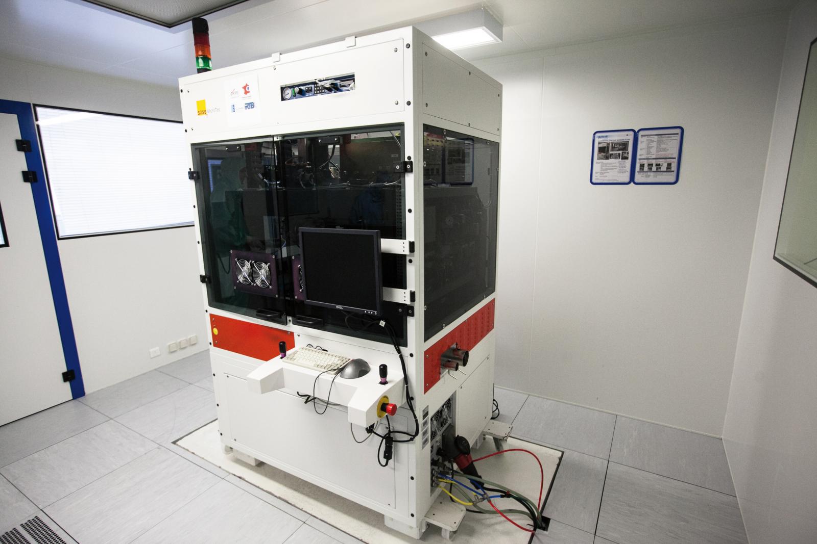
Megasonic wafer Cleaner & Wafer bonding inspection systems
| CL200 & IR200 | Use: > Final rinsing of wafers before bonding (reduction of particles) |
 |
Technical specifications |
——
Plasma Surface activation system
| Nanoprep NP12 |
Use: > Surface activation for low-temperature bonding applications |
 |
Technical specifications |
——
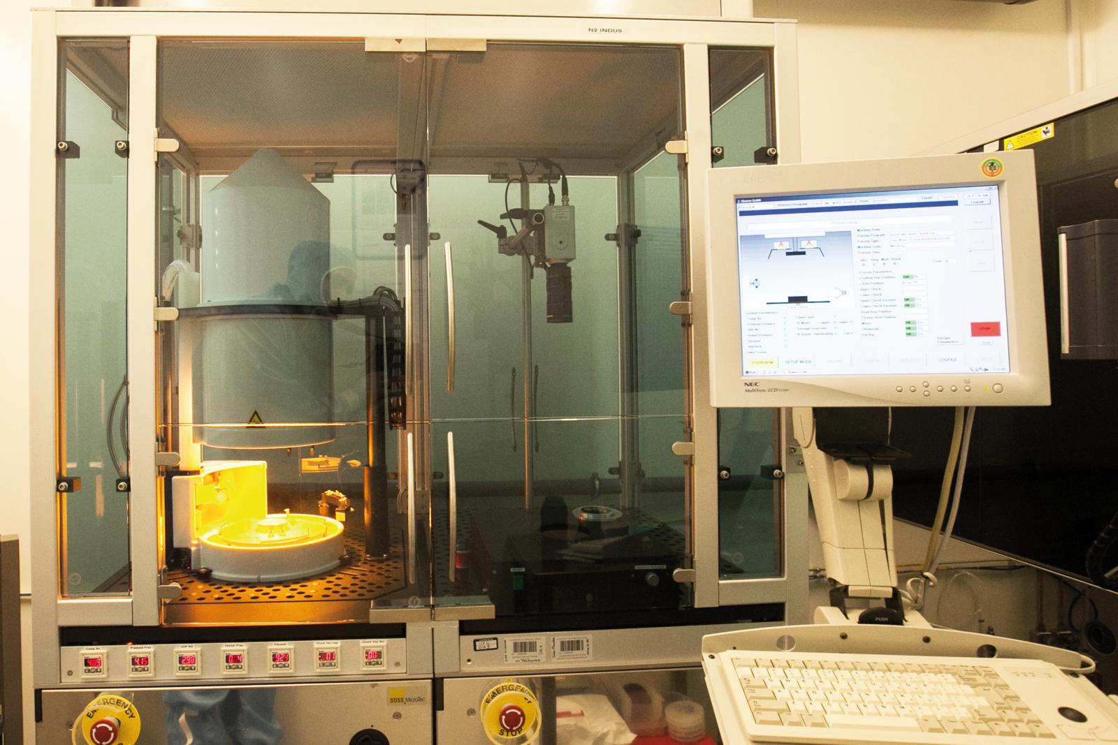
Multi-wafer bonder
| EVG 501 |
Use: > Special bonding process (Anodic, Eutectic, Thermo-Compression, Adhesive & Direct) |
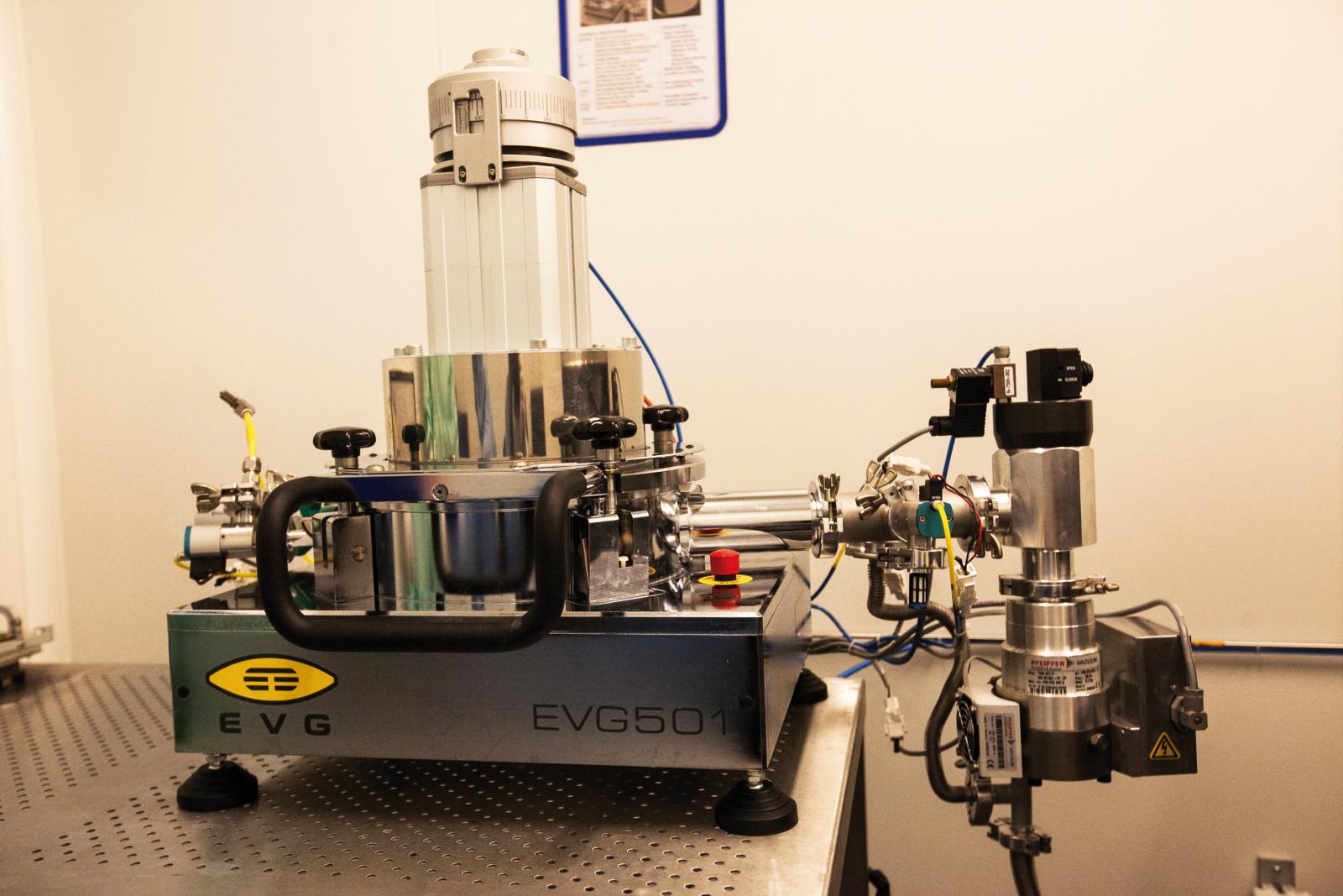 |
Technical specifications |
——
Multi-wafer bonder
| AML 402P |
Use: > Special bonding process (Anodic, Eutectic, Thermo-Compression & Direct) |
 |
Technical specifications |
——
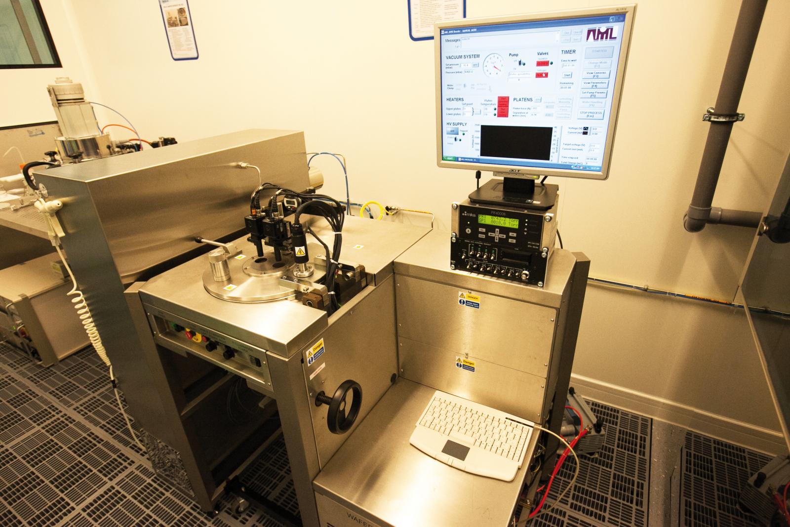
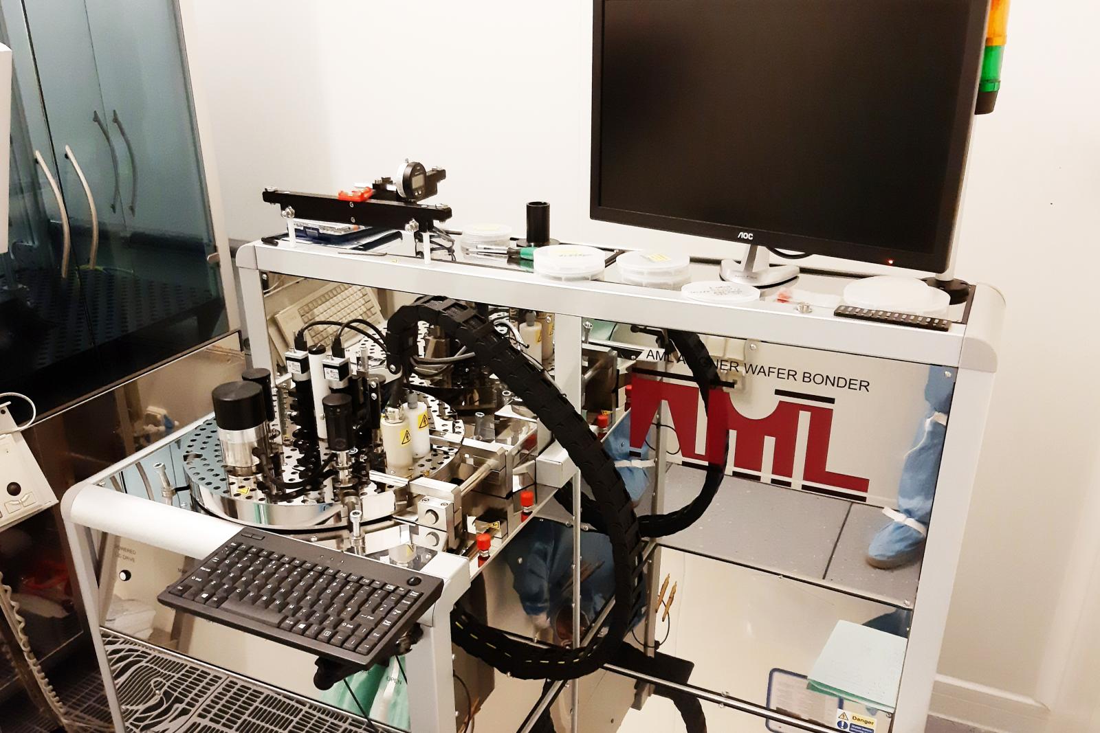
Wafer aligner-bonder 6’’
| AML AWB-04 |
Use: > Flexible automatic multi-process system > No flags clamping |
 |
Technical specifications |
——
Automatic Flip-chip bonder
| Süss Microtec FC250 |
Use: > Die to substrate bonding and interconnecting |
 |
Technical specifications |
——
Pick and Place Die Bonder
| TPT HB-70 |
Use: > Die bonding > Assembly of micro-components |
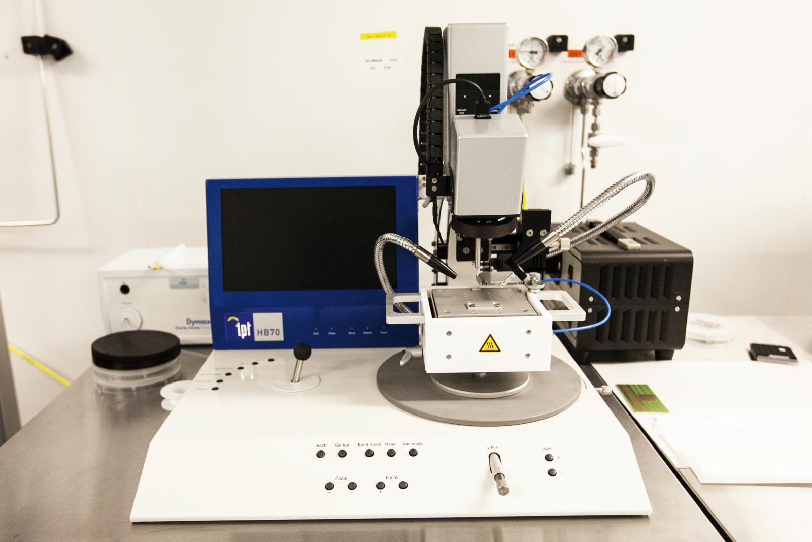 |
Technical specifications |
——
Semi-Automatic Wire Bonder
| TPT HB-16 |
Use: > Wire bonding of electronic components |
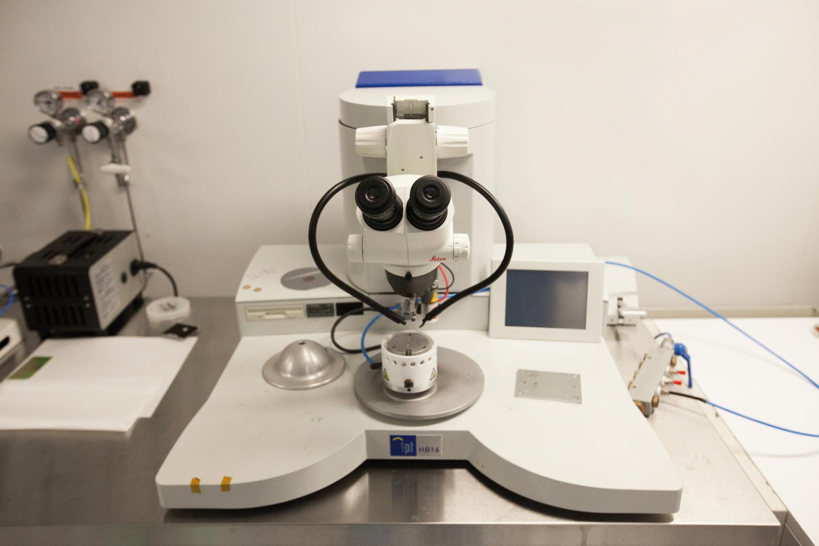 |
Technical specifications |
——
Mechanical micro bond tester
| Nordson DAGE 4000 Plus |
Use: >Testing of Electrical interconnects & Bonding quality |
 |
Technical specifications |
——
Packaging overview
——
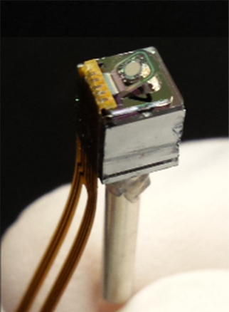
Realisations
|
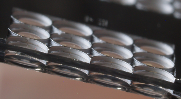
(Si-Glass-Si-Glass, anodic bonding) |
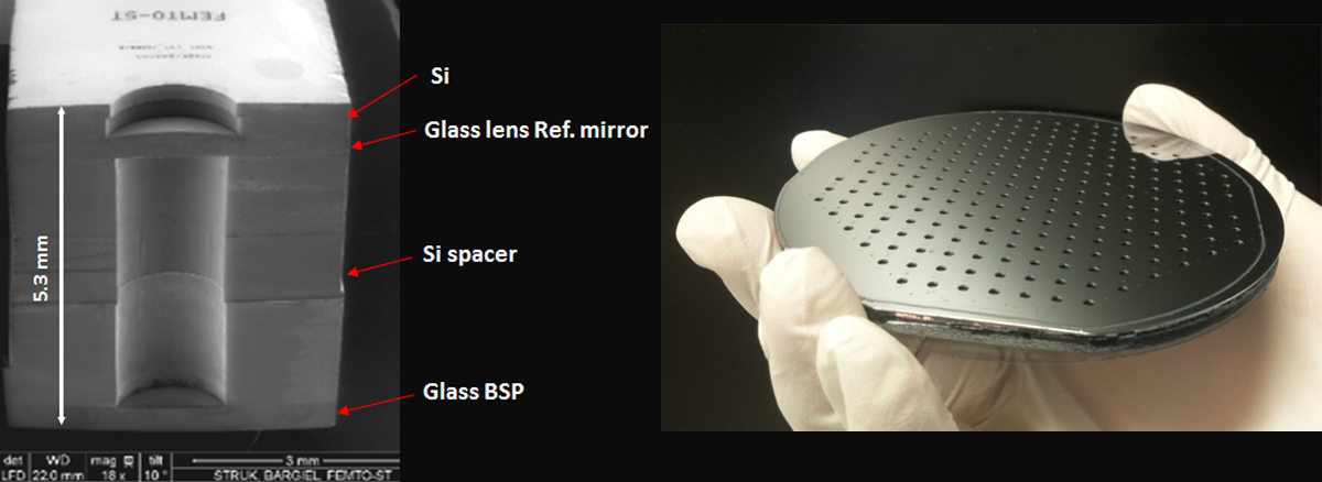
(Si-Glass-Si-Glass, 5.3mm thick, anodic bonding)
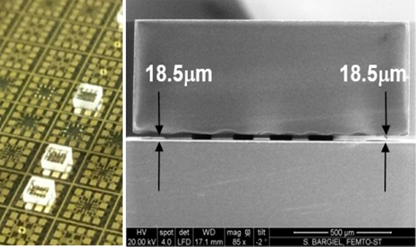
(1.7x1.7x0.5mm3) |
|
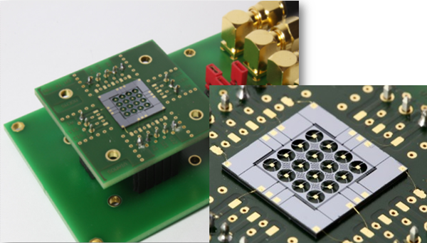
(adhesive bond on PCB and Au wire bonding) |
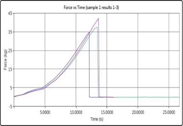
(PULL or SHEAR mode) |