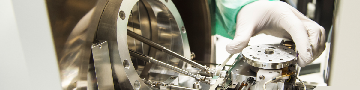
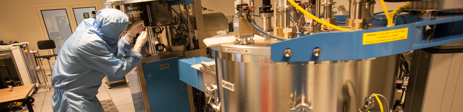
Thin film technology
The technological center MIMENTO offers a special resource dedicated to thin film deposition of metals, oxides and other compound materials. The deposited thicknesses may vary from few nanometers
to a couple of micrometers, depending on the deposited material and the technique used.
Generally, the methods used to deposit thin films are split into two categories: Physical Vapor Deposition (PVD) and Chemical Vapor Deposition (CVD). The distinguishing feature between PVD and CVD techniques is in the vapor. In PVD, the vapor is made up of atoms and molecules that condense on the substrate, and for CVD, the vapor undergoes a chemical reaction on the substrate which results into a thin film.
Within FEMTO-ST it exists three deposition techniques for the thin film deposition:
- Sputtering (PVD)
- Evaporation (PVD)
- Plasma enhanced CVD
Furthermore, MIMENTO has the possibility to perform thermal treatments. The purpose of thermal treatments are various, in order to affect their optical, electrical and mechanical properties.
- Reduce or eliminate the residual stress in thin films
- Densify deposited films
- Activation/diffusion of dopants
- Recrystallization of the samples
The RTP system is a single wafer processing, performing annealing at elevated temperatures in a short time (the order of few minutes). The conventional furnace is capable to process lot of wafers at a time with thermal cycles of the order of several hours. The multitube system allows to dedicate one of the tube to process wet or dry oxidation.
Resource contact:
| Stefania OLIVERI 03 81 66 63 02 stefania.oliveri [at] femto-st.fr | Personal page: https://www.femto-st.fr/fr/personnel-femto/stefaniaoliveri |
| Matthieu MICOLLE 03 63 08 26 27 matthieu.micolle [at] femto-st.fr | Personal page: https://www.femto-st.fr/fr/personnel-femto/matthieumicolle |

RF magnetron sputtering system
| Plassys MP 450S | Use: > Metal, Oxide & Nitride deposition |
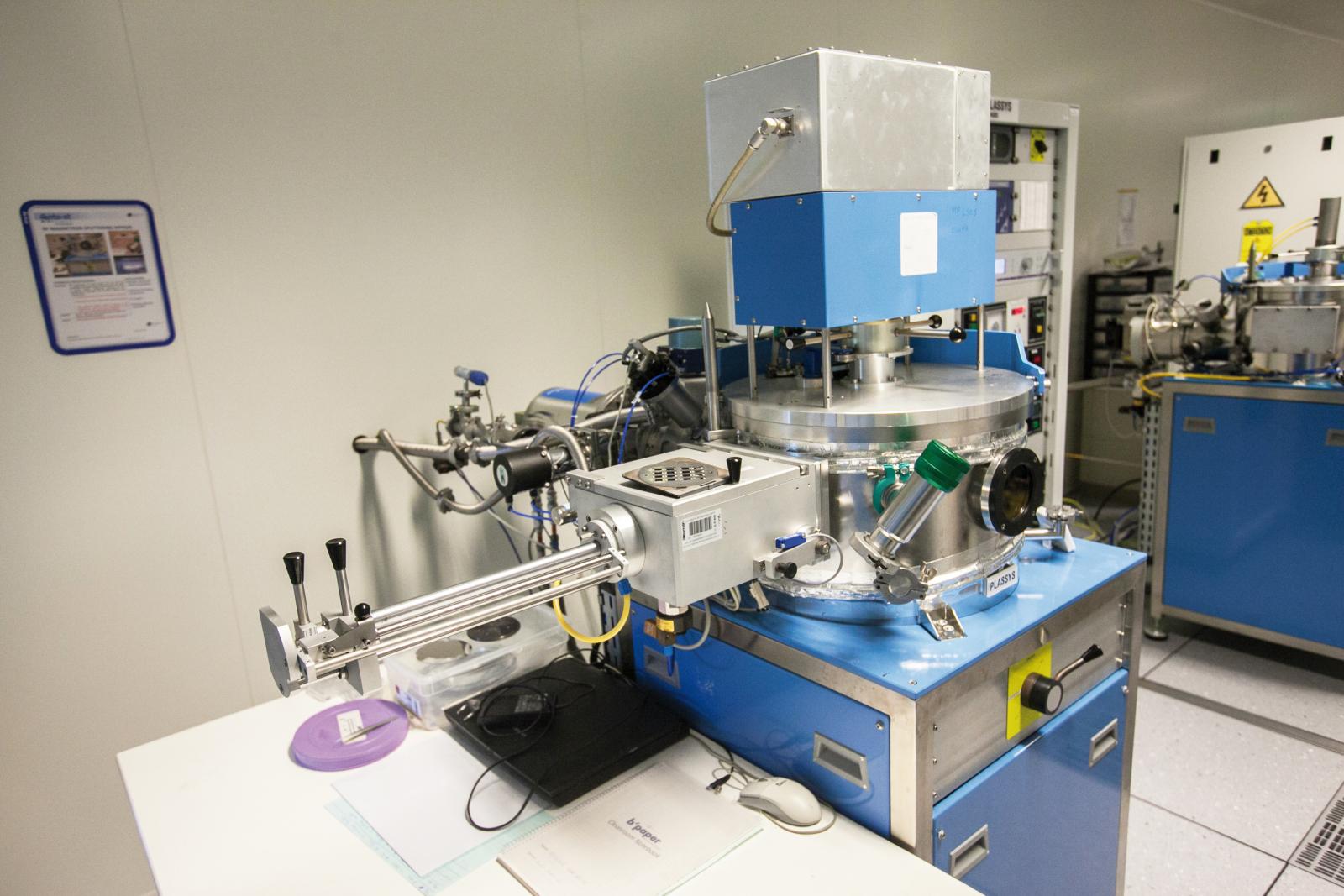 | Technical specifications |
——
DC magnetron sputtering system
| Alliance Concept DP650 | Use: > Metal deposition |
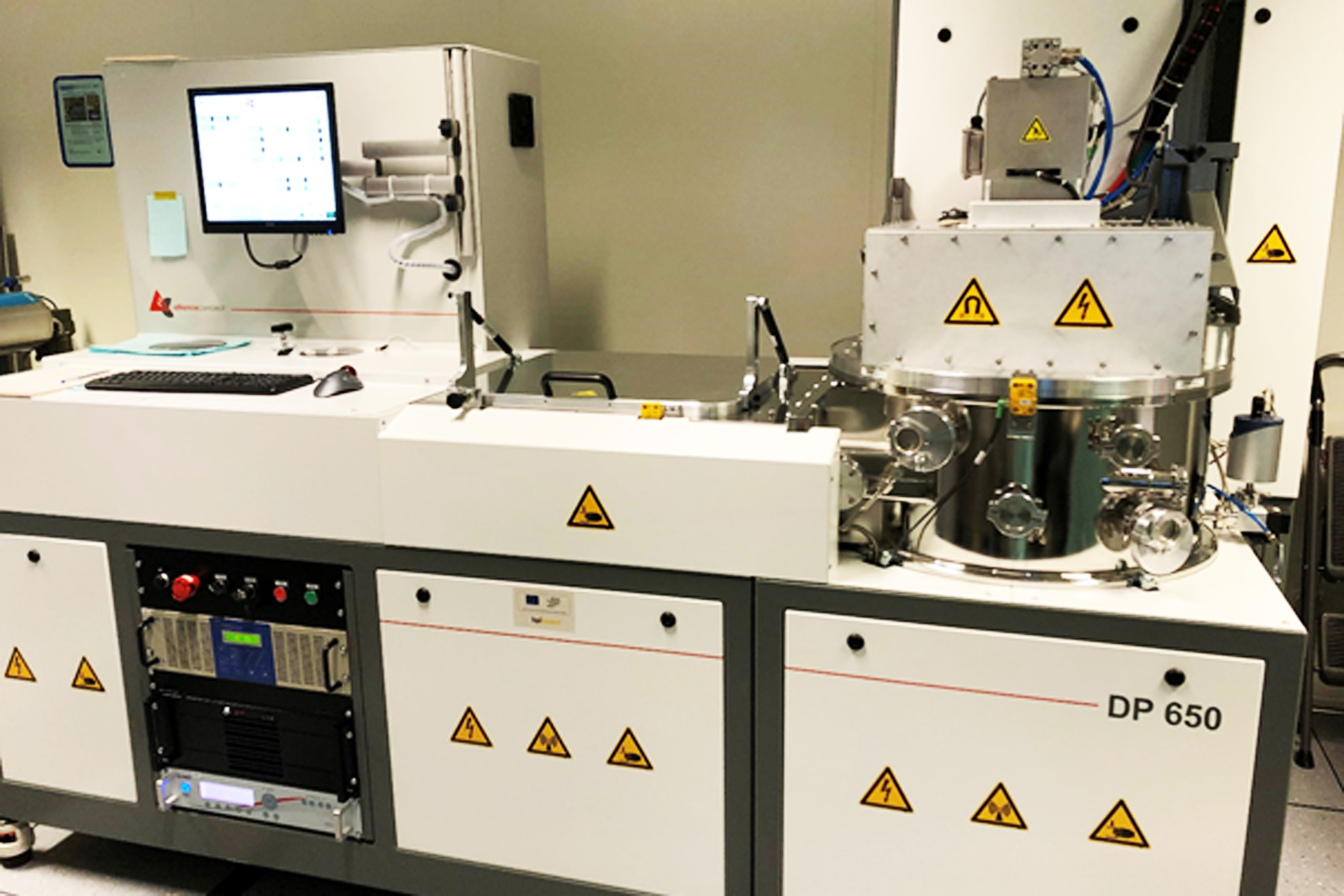 | Technical specifications |
——
DC magnetron sputtering system
| Plassys MP 500 | Use: > Metal deposition |
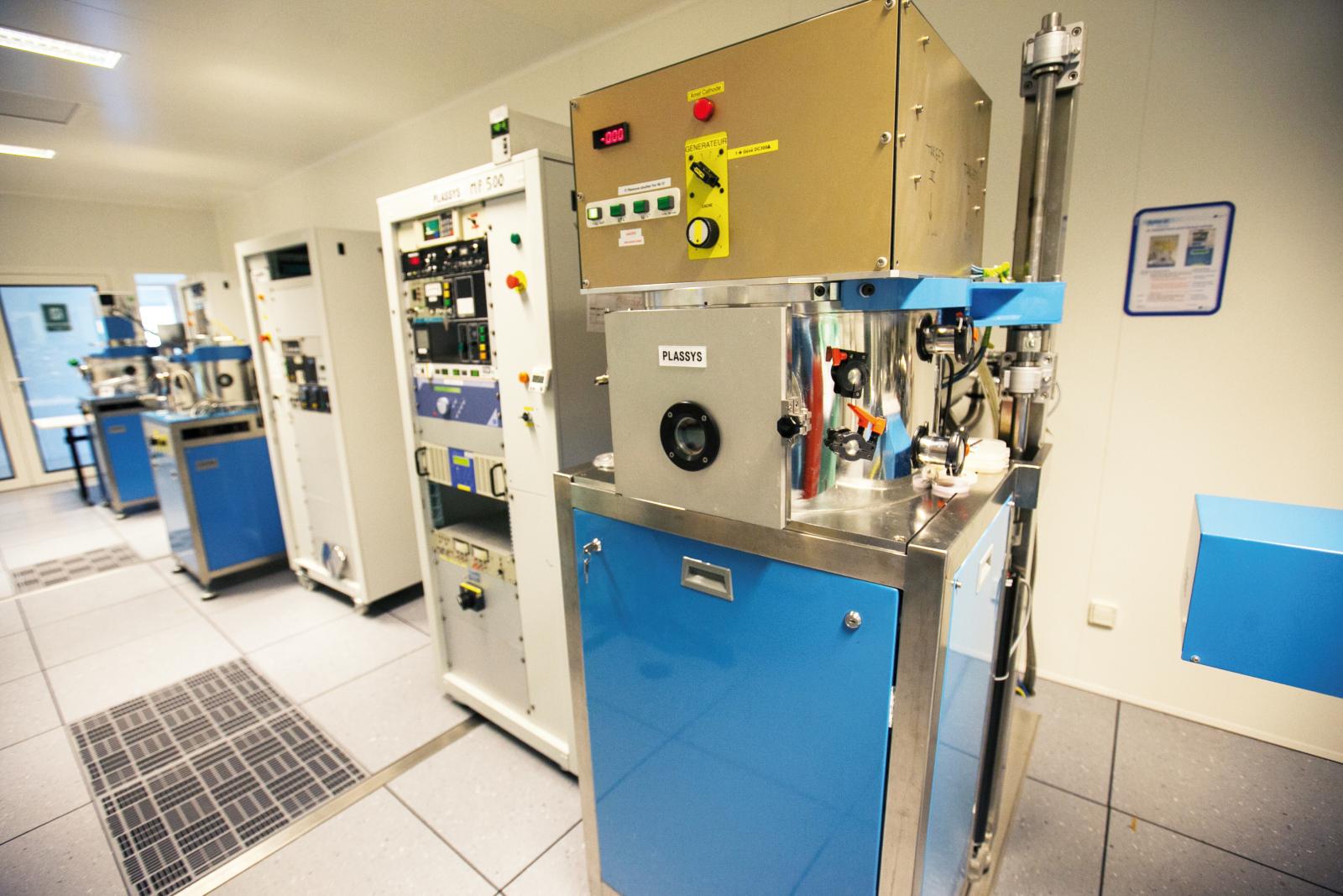 | Technical specifications |
——
DC magnetron sputtering system
| Plassys MP 700S | Use: > Metal deposition |
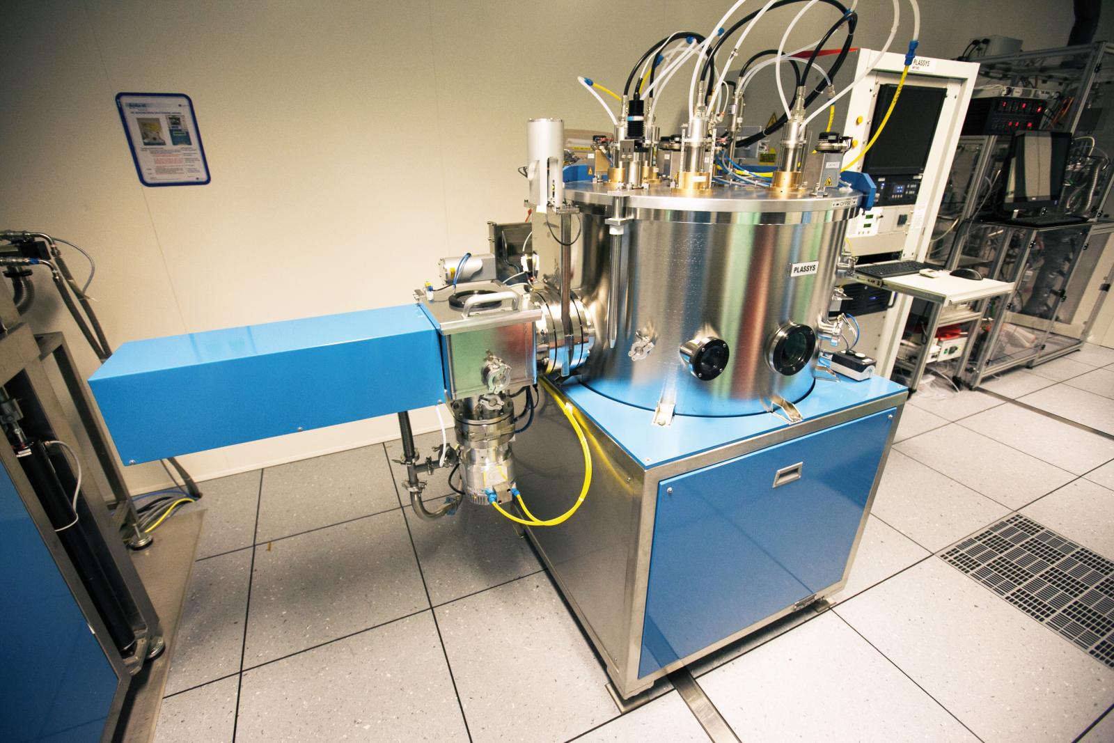 | Technical specifications |
——
Plasma enhanced atomic layer deposition
| Veeco Fiji G200 | Use: > Highly conformal and uniform oxide and platinum depositions |
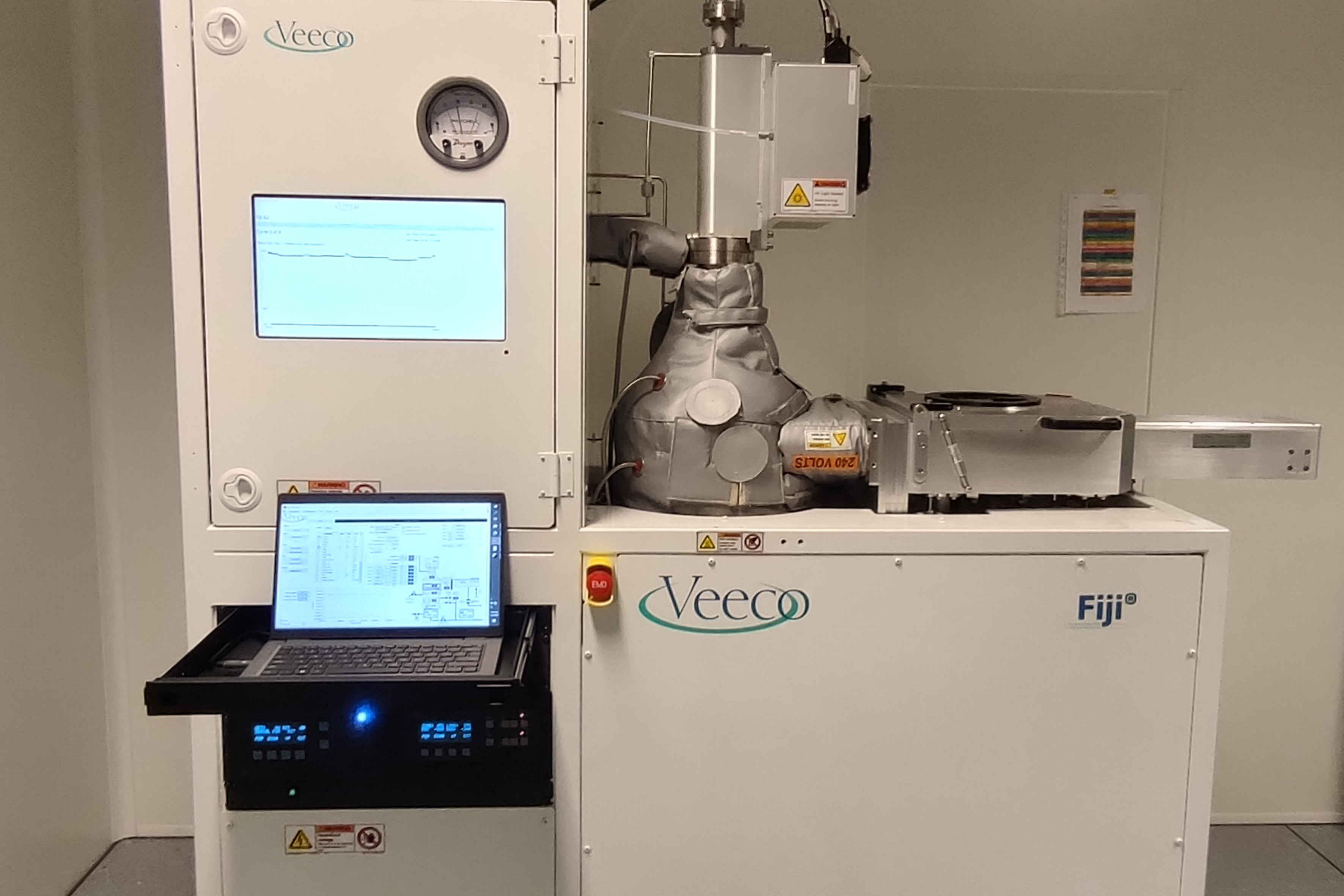 | Technical specifications |
——
Electron-beam evaporator
| Alliance Concept EVA 450 | Use: > Metal deposition for lift-off processes |
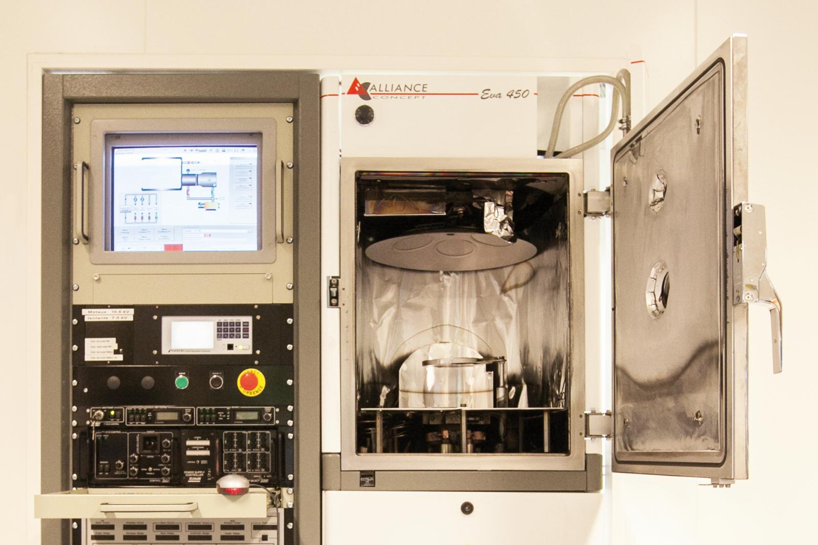 | Technical specifications |
——
Electron-beam evaporator
| Plassys MEB 600 | Use: > Metal & Oxide deposition for lift-off processes |
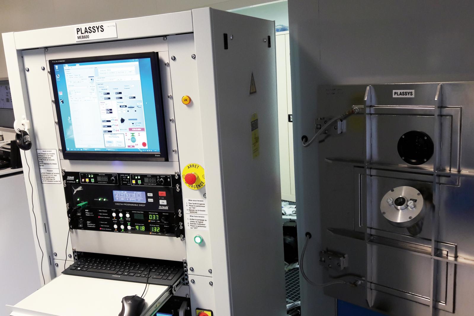 | Technical specifications |
——
ICPECVD
| Sentech SI 500D | Use: > Oxide & Si3N4 deposition > Good conformal deposition |
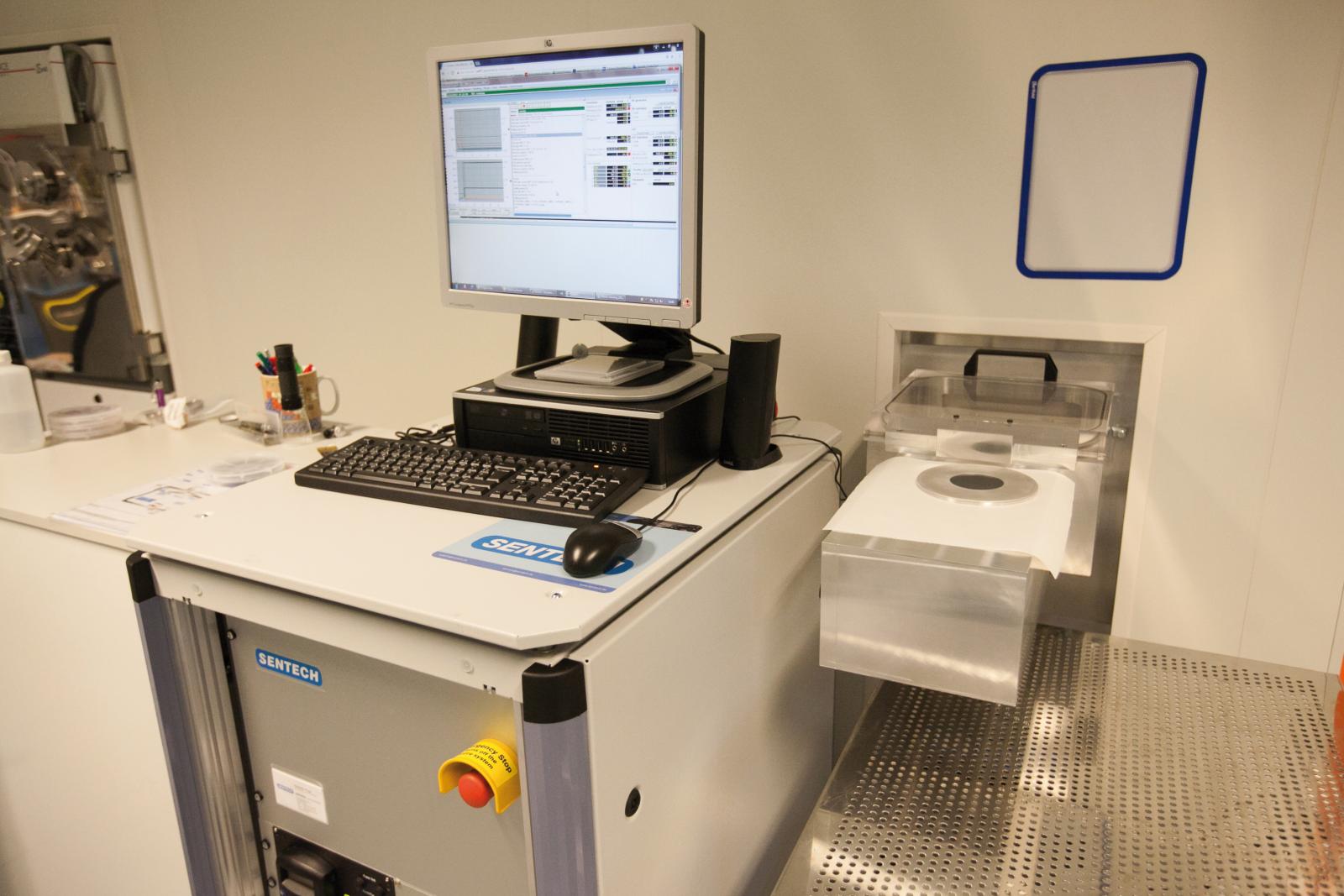 | Technical specifications |
——
Oxidation and annealing furnace
| AET | Use: > Thermal oxidation & diffusion |
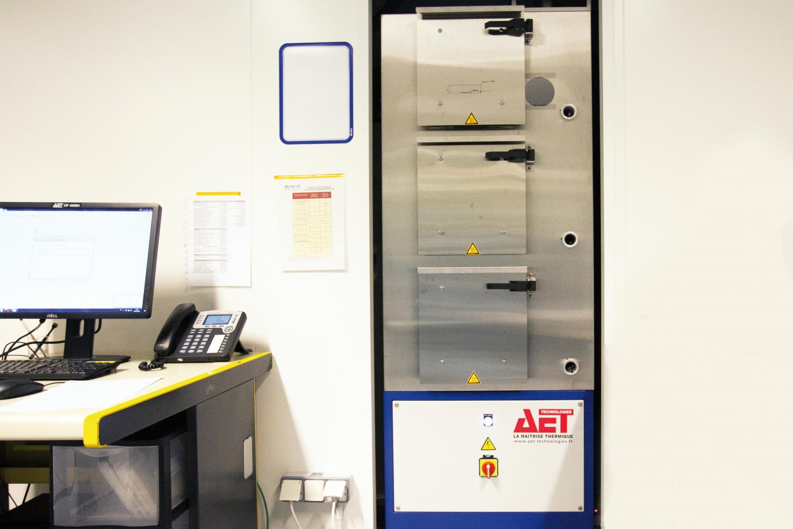 | Technical specifications |
——
Rapid thermal processing
| Annealsys AS-Premium RTP | Use: > Densification & Crystallization > Contact annealing |
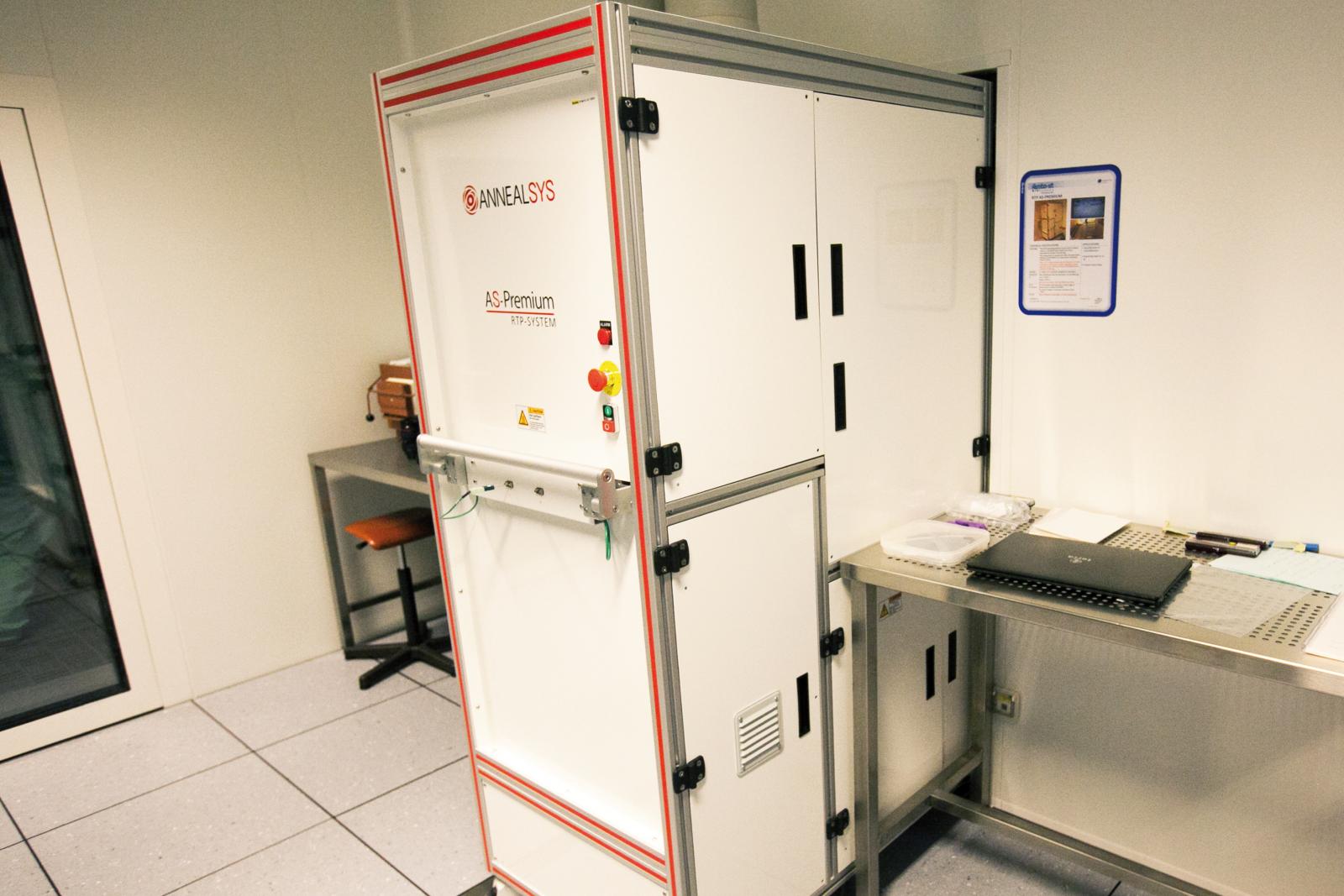 | Technical specifications |
——
Thin film overview
——
Realisations
 Gold terrace for proteomics Gold terrace for proteomics |  Multi-layer acoustic wave mirror Multi-layer acoustic wave mirror |
 Optical fiber tip coating Optical fiber tip coating |  Resonant structures excited by piezoelectric ZnO thin film Resonant structures excited by piezoelectric ZnO thin film |